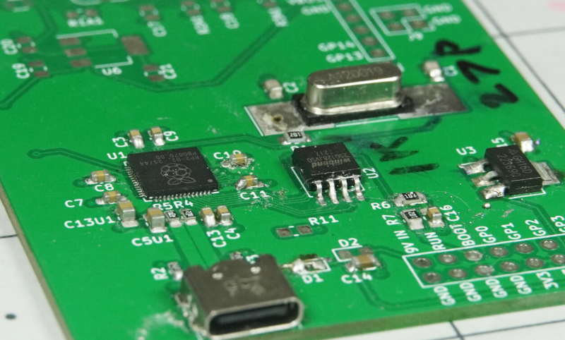
Building a custom RP2040 board looks deceptively easy. The chip is affordable, the Raspberry Pi Pico is everywhere, and the internet is packed with friendly schematics that whisper, “Come on, how hard could this be?” Then your shiny purple PCB arrives, you plug it into USB, and absolutely nothing happens. No drive appears. No LED blinks. Your computer stares back like you just plugged in a cracker.
This guide is about how not to build an RP2040 board. In other words, it is a tour of the common mistakes that turn a promising microcontroller PCB into an expensive drink coaster. The RP2040 is a powerful dual-core Arm Cortex-M0+ microcontroller with 264 KB of SRAM, USB support, programmable I/O, and external QSPI flash execution. But it is not magic. It still needs clean power, good routing, a working clock, sane boot circuitry, and a layout that respects physics.
If you are designing a Raspberry Pi RP2040 custom PCB, think of this article as the checklist your future self wishes you had taped to your monitor before clicking “Order boards.”
Why RP2040 Board Design Goes Wrong So Easily
The RP2040 invites experimentation because it is flexible. That same flexibility is also where many mistakes begin. Unlike simple hobby modules where most critical parts are already handled, a bare RP2040 design asks you to make decisions about power regulation, flash memory, USB routing, boot mode, reset access, crystal or oscillator selection, SWD debugging, and manufacturability.
A Raspberry Pi Pico hides all of that behind a friendly board edge. Your own RP2040 board does not. Once you leave the warm blanket of the Pico, every missing capacitor and every “I’ll fix that in firmware” assumption becomes your problem.
Do Not Start by Deleting the Reference Design
The first wrong move is opening the official hardware design files, admiring them for twelve seconds, and then rebuilding everything from memory because your design is “minimal.” Minimal is a dangerous word in PCB design. Sometimes it means elegant. Sometimes it means “the board only works when held at a 37-degree angle under a full moon.”
The official RP2040 hardware design guide, datasheet, and Raspberry Pi Pico design files exist for a reason. They show working decisions for flash, USB, power, clocking, decoupling, and boot behavior. You do not need to copy every feature, but you should understand every part before removing it. If a component seems unnecessary, ask: “What problem was this solving?” before you evict it from the schematic like a bad roommate.
Bad example
You remove several capacitors, the reset access, the BOOTSEL button, and the SWD header because “space is tight.” The board arrives, fails to enumerate over USB, and now your debugging method is squinting.
Better approach
Begin with a known-good minimal RP2040 schematic. Remove features only after you understand their purpose, and leave test pads whenever you are unsure.
Do Not Treat Power as an Afterthought
The RP2040 needs more than “some 3.3V somewhere.” It uses 3.3V for I/O and an internal regulator arrangement for the 1.1V core supply. The power system needs proper decoupling, short paths, and stable regulation. A board can show 3.3V on a multimeter and still fail because the rail is noisy, slow to rise, or poorly decoupled at the pins.
One of the most common RP2040 PCB mistakes is placing decoupling capacitors wherever they fit instead of where they work. Decoupling capacitors are not decorative ceramic confetti. They must sit close to their respective power pins with short, low-inductance paths to ground.
What not to do
Do not place all capacitors in a neat row across the board because it looks tidy. Electrons do not care about your aesthetic grid. They care about loop area, impedance, and distance.
What to do instead
Place local 0.1 µF capacitors close to the RP2040 power pins, use the recommended bulk capacitors, and keep the 3.3V and 1.1V paths short and wide. Give the board a solid ground reference. If you are using USB power, battery power, or multiple power inputs, design the power path deliberately instead of hoping the smoke stays inside.
Do Not Route USB Like a Garden Hose
USB looks simple on a schematic: D+, D-, maybe a connector, done. On a PCB, USB is less forgiving. The RP2040 supports USB device and host functionality, but your layout still needs to respect differential routing, impedance, short paths, ESD protection decisions, and connector orientation.
For full-speed USB, you have more tolerance than high-speed USB, but that does not mean you should route D+ around the board like it is taking the scenic route while D- goes straight home. Keep the pair close together, avoid unnecessary vias, maintain similar lengths, and place series resistors or protection components according to a proven reference design.
The classic USB-C trap
USB-C is wonderful until you forget the configuration-channel resistors. A USB-C receptacle used as a device usually needs the correct pull-down resistors on CC1 and CC2 so the host knows something is attached. Skip them and your beautiful USB-C connector may become a stylish charging-shaped hole.
Do Not Forget BOOTSEL and Reset Access
The RP2040’s ROM bootloader is one of its best features. With the correct BOOTSEL behavior, the chip can appear as a USB mass-storage device so you can drag and drop firmware. But this convenience depends on your board allowing the right boot condition at reset.
A surprising number of custom RP2040 boards become difficult to program because the designer did not include a convenient BOOTSEL button, reset button, jumper, or accessible test pad. Technically, you may not need a dedicated button in every final product. Practically, you will want one during bring-up unless you enjoy unplugging USB cables like a medieval troubleshooting ritual.
Good design habit
Add both reset and BOOTSEL access during prototypes. If the final product cannot fit buttons, use test pads or solder jumpers. Your first board revision is not the place to be heroic.
Do Not Treat External Flash as Optional
The RP2040 uses external flash for program storage through its dedicated QSPI interface. The chip can execute code in place from external flash, but that flash must be wired correctly, powered correctly, and supported by the boot process.
Common flash mistakes include using an incompatible part, routing QSPI lines too long, omitting needed pull-ups, mixing up pins, or placing the flash far from the microcontroller. The QSPI flash is not a casual peripheral hanging out at the edge of the board. It is where your program lives. Treat it like the brain’s pantry, not an afterthought.
Layout advice
Keep QSPI traces short and direct. Place the flash close to the RP2040. Avoid routing noisy signals under or between flash lines. Check the flash package footprint carefully, especially if you are swapping between similar-looking WSON, SOIC, or USON packages.
Do Not Guess on the Clock Circuit
Clocking issues are sneaky. A bad crystal circuit may not fail dramatically; it may boot sometimes, disappear from USB randomly, or behave differently depending on temperature, cable, or whether your hand is near the board. That is the kind of bug that makes engineers start bargaining with desk lamps.
The RP2040 commonly uses a 12 MHz crystal circuit, but a crystal is not just “a shiny two-pin timing rock.” Load capacitance, trace length, grounding, component placement, and startup behavior matter. Some designers choose an external oscillator module to simplify clocking, while others follow the reference crystal circuit carefully. Either can work. Guessing rarely does.
What not to do
Do not put the crystal far from the chip. Do not route high-speed digital traces under the crystal. Do not choose random load capacitors because they were already in your parts bin. And do not assume a crystal footprint is correct because the symbol looked friendly.
Do Not Hide the SWD Pins
USB bootloading is convenient, but SWD debugging is your escape hatch when firmware, boot mode, or USB behavior goes sideways. The RP2040 supports Serial Wire Debug, and adding SWD pads or a small connector can save hours of guesswork.
Even if your final board will never expose debug pins to users, your prototype should. At minimum, break out SWDIO, SWCLK, ground, and reset access. A board without debug access is like a car with the hood welded shut. Stylish, perhaps. Unhelpful, definitely.
Do Not Ignore the Ground Plane
A poor ground layout can make a technically correct schematic behave like a haunted appliance. The RP2040 has fast digital edges, USB signaling, flash activity, and possibly ADC inputs all sharing the same board. A clean ground strategy matters.
Use a solid ground plane whenever possible. Keep return paths short. Avoid slicing the ground plane under USB, crystal, or QSPI traces. If you have analog inputs, think carefully about reference stability and noisy neighbors. The ADC will happily measure your bad layout decisions and report them as “sensor data.”
Do Not Make the Board Impossible to Assemble
The RP2040 package is not impossible to solder, but it is not a beginner-friendly through-hole resistor either. It uses a fine-pitch QFN package with an exposed pad. Your PCB footprint, solder mask expansion, paste aperture, thermal relief, and assembly method all matter.
If you are hand-assembling, be realistic. If you are using an assembly service, check part availability, orientation, package variants, and manufacturer part numbers. Many first revisions fail not because the circuit concept was wrong, but because one footprint was mirrored, one regulator package was mismatched, or one flash chip was out of stock and replaced with a “similar” part that was not similar enough.
Prototype-friendly tip
Add test pads for 3.3V, 1.1V, ground, reset, BOOTSEL, USB D+, USB D-, flash chip select, and SWD. Test pads are cheap. Mystery is expensive.
Do Not Skip ERC, DRC, and Peer Review
Before ordering PCBs, run electrical rule checks and design rule checks. Then inspect the board manually. Then, ideally, ask someone else to inspect it. Your brain is excellent at not seeing the same mistake for three consecutive evenings.
Look for swapped USB data lines, missing power labels, unconnected ground pins, wrong connector orientation, mismatched footprints, shorted thermal pads, missing pull-ups, and nets that accidentally share a name. Zoom in until the board looks ridiculous. That is where the gremlins live.
Do Not Bring Up the Board Randomly
When the board arrives, do not immediately plug it into your favorite laptop and hope for fireworks of success. Bring-up should be calm and boring, which is exactly what you want when electricity is involved.
A sane RP2040 bring-up sequence
- Inspect the bare PCB for manufacturing defects.
- Check component orientation before powering anything.
- Measure resistance between power rails and ground.
- Power the board from a current-limited supply first.
- Verify 3.3V and 1.1V rails.
- Check reset behavior.
- Test BOOTSEL mode over USB.
- Try SWD connection if USB does not enumerate.
- Program a simple blink test before running complex firmware.
If you skip these steps, you are not saving time. You are converting debugging into performance art.
Do Not Assume Firmware Can Fix Hardware
Firmware can work miracles, but it cannot reroute USB traces, add a missing capacitor, rotate a QFN package, or solder a forgotten pull-down resistor onto a sealed enclosure. Hardware bugs become especially painful because every fix may require knives, wires, microscopes, or a new PCB order.
Design your RP2040 board so firmware has a fair chance. Give it stable power, a working boot path, correct flash, good clocking, debug access, and clean signals. Then firmware can do the fun part instead of compensating for preventable chaos.
Experiences and Lessons from Building RP2040 Boards the Wrong Way
The most useful RP2040 design lessons often arrive disguised as failure. A board that refuses to enumerate over USB teaches more about routing and boot circuitry than ten perfect tutorials. The trick is to learn the lesson before ordering revision five.
One common experience is the “power rails look fine” trap. You measure 3.3V and 1.1V with a multimeter and assume the power system is innocent. But the RP2040 may still be unhappy because the rail dips during startup, the decoupling path is too long, or the regulator behaves poorly under transient load. A multimeter gives you the weather report, not the security-camera footage. For deeper diagnosis, use an oscilloscope if available, especially during plug-in and reset.
Another painful lesson involves USB connectors. Many designers switch from micro-USB to USB-C because USB-C feels modern and professional. Then the board does not connect because the CC resistors are wrong or missing. The connector was not the problem; the assumption was. USB-C is not just a reversible version of older USB. It has detection rules, and your schematic must participate in the conversation.
Clock circuits also create memorable headaches. A crystal placed too far from the RP2040, paired with the wrong capacitors, or surrounded by noisy traces may work on one unit and fail on another. That kind of intermittent behavior is worse than a clean failure because it tempts you to blame software, cables, the operating system, your soldering iron, and possibly Mercury in retrograde. In reality, the oscillator circuit wanted careful placement from the beginning.
Flash mistakes are equally educational. The RP2040 depends on external QSPI flash for normal code storage. If flash is wired incorrectly, the chip may still enter ROM bootloader mode, which can mislead you into thinking the board is basically fine. But once you try to run firmware, nothing works. Always verify the flash part, footprint, orientation, chip-select behavior, and QSPI trace routing before manufacturing.
Then there is the lesson of debug access. The first time you build a board without SWD pads, you may feel clever because you saved space. The first time that board fails, you will feel less clever. Debug pads do not need to be pretty. They need to exist. Even tiny pogo-pin pads can turn a dead-looking board into a solvable problem.
The final experience is emotional: do not take a failed RP2040 board personally. Every hardware designer has a private museum of mistakes. The goal is not to avoid all errors forever; the goal is to make errors cheaper, easier to diagnose, and less likely to repeat. Add labels. Add test points. Keep notes. Compare against working boards from Raspberry Pi, Adafruit, SparkFun, and other proven designs. When something fails, write down the symptom, measurement, fix, and lesson. Future-you will read those notes like ancient treasure maps.
In short, building an RP2040 board badly is easy. Building one well is also achievable, but it requires respect for the boring details: power, ground, clock, flash, USB, reset, boot, layout, and test access. The board does not need to be overbuilt. It needs to be understandable, measurable, and honest.
Conclusion
Learning how not to build an RP2040 board is one of the fastest ways to learn how to build one correctly. The big mistakes are rarely mysterious: skipping the reference design, weakening the power system, abusing USB routing, hiding BOOTSEL and reset, mishandling QSPI flash, guessing on the crystal circuit, and leaving yourself no SWD debug path.
The RP2040 is a generous chip, but it is not a substitute for good engineering habits. Start from proven documentation. Keep critical traces short. Place decoupling capacitors where they belong. Make boot and reset accessible. Add test pads. Review the design before ordering. Bring the board up slowly. Your reward is a custom RP2040 PCB that behaves like a product instead of a puzzle box.
And if the first revision still fails? Congratulations. You are officially doing hardware. Take notes, patch carefully, and let revision two be smarter.